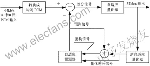
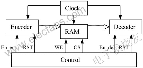
ADPCM algorithm and its codec principle This article refers to the address: http:// ADPCM (Adaptive Differential Pulse Code Modulation) combines the adaptive characteristics of APCM and the differential characteristics of DPCM system, and is a better waveform coding. Its core idea is: use adaptive to change the size of the quantization step, that is, use small quantization steps to encode small differences, use large quantization steps to encode large differences; use past sample values ​​to estimate the next input sample. The predicted value is such that the difference between the actual sample value and the predicted value is always the smallest. The quantized value recorded by ADPCM is not the amplitude of each sample point, but the difference between the amplitude of the point and the amplitude of the previous sample point. ADPCM is a waveform coding technique that uses a high correlation between samples and samples and quantization step adaptation to compress data. The ADPCM standard is a transcoding system that uses ADPCM conversion techniques to achieve a 64 kb/s A-law or u-law PCM (Pulse Code Modulation) rate and a 32 kb/s rate conversion. A simplified block diagram of ADPCM is shown in Figure 1. The input signal of the ADPCM codec is G.711 PCM code, the sampling rate is 8 kHz, and each code is represented by 8 bits, so its data rate is 64 kb/s. The output code of ADPCM is the output of "adaptive quantizer". The output is a differential signal represented by 4 bits. Its sampling rate is still 8 kHz, and its data rate is 32 kb/s, thus obtaining 2:1. Data compression. Overall structure of the circuit Based on the ADPCM algorithm, the speech codec VLSI chip can be divided into several modules of encoding, decoding, storing, controlling and clocking. The encoding module implements a data compression function, and converts the input PCM signal into an ADPCM code; the storage module saves the encoded ADPCM code under the action of the control module; the decoding module implements a decompression function, converts the ADPCM code into a PCM code; and the control module The function is to control the coordination of other modules; the clock module mainly divides the original clock signal of the external crystal to obtain the actual clock signal required by the circuit system. The overall structure of the circuit is shown in Figure 2, where En_en and En_de are the enable signals for encoding and decoding, respectively, and RST is the reset signal. When WE is "1", the RAM write is valid, and when WE is "0", the RAM read is valid, and when CS is "1", the RAM can be written or read. (a) ADPCM encoder (b) ADPCM decoder Figure 1 ADPCM simplified block diagram Circuit design process This paper uses the Top-down method for circuit design. The main design flow is as follows: Firstly, based on Verilog HDL, Active-HDL is used to perform RTL level description and function simulation of the circuit; the program with correct function simulation is integrated and adapted in the Quartus II development system; the next netlist file will be obtained. (.vo) and the anti-standard file with delay information (.sdo) are loaded into ModelSim SE, and the corresponding device library of the selected device is added for timing simulation. After the timing simulation is passed, the Quartus II is obtained by "*.sof". The file is downloaded to the FPGA through the JTAG configuration mode for actual test without power-down. The "*.pof" file can also be downloaded to the FPGA through the AS configuration mode for actual power-down testing. The top level of the circuitry is as follows. Figure 2 Overall structure of the circuit Module ADPCM_TOP (PCM_OUT, PCM_IN, RECORD, PLAY, CLK, CLK8K); Parameter ADDR_WIDTH=14; Parameter PCM_WIDTH=8; Input [PCM_WIDTH-1:0] PCM_IN ; Wire [PCM_WIDTH-1:0] PCM_IN ; Output [PCM_WIDTH-1:0] PCM_OUT ; Wire [PCM_WIDTH-1:0] PCM_OUT ; Input CLK, RECORD, PLAY; Output CLK8K; Wire[3:0] code_in,code_out; Wire en_encoder, en_decoder, re_rst, pl_rst, WE, CS, CLK_8K; Wire [ADDR_WIDTH-1:0] ADDRESS; Assign CLK8K =CLK_8K; CLOCK_GE U0 (CLK, RECORD, CLK_8K); Encoder_new U1 (PCM_IN, re_rst, en_encoder, CLK_8K, code_in); RAM U2 (ADDRESS, WE, CS, CLK_8K, code_in, code_out); Decoder_new U3 (pl_rst, CLK_8K, code_out, en_decoder, PCM_OUT); Controllogic U4 (CS, re_rst, pl_rst, en_encoder, en_decoder, WE, ADDRESS, RECORD, PLAY, CLK_8K); Endmodule Submodule circuit design and simulation The entire speech codec VLSI chip includes an encoding circuit, a decoding circuit, a storage circuit, a control circuit, and a clock circuit. The design of the critical circuit is specifically described below. 1 coding circuit The encoding circuit implements a data compression function, converts the input PCM signal into a uniform PCM code, and then differentiates it from the prediction signal, and the obtained differential signal is compression-encoded by an "adaptive quantizer" to obtain an ADPCM code, and the ADPCM code is returned through " The inverse adaptive quantizer" and the "adaptive predictor" are used to construct the next prediction signal. The simulation circuit simulation waveform is shown in Figure 3, where PCM_IN is the encoder input signal (PCM code) and CODE is the output signal (ADPCM code) obtained after encoding. Figure 3 coding circuit simulation waveform 2 decoding circuit The decoding circuit implements a decompression function, and the ADPCM code is subjected to an "inverse adaptive quantizer" to obtain a quantized differential signal, and the quantized differential signal is added to the predicted value to obtain a reconstructed signal, which is then converted into a PCM code. The decoding circuit simulation waveform is shown in Fig. 4, where CODE is the decoder input signal (ADPCM code), and PCM_OUT is the output signal (PCM code) obtained after decoding. Compared with the PCM_IN before the codec in Fig. 3, it can be seen that the decoding error is small. 3 other modules The control circuit controls the coordination of other circuit modules, and enables the memory write signal at the same time of encoding, so that the output data of the encoding circuit can be stored in the memory in time; while the memory is read out while decoding, the encoding and decoding cannot be performed simultaneously. The clock circuit mainly divides the original clock signal of the external crystal oscillator to obtain the clock signal actually needed by the circuit system. The external crystal oscillator used in this system has a natural frequency of 14.318MHz. After dividing by frequency, an 8kHz clock can be obtained. The storage circuit saves the encoded ADPCM code (32 kb/s) under the action of the control circuit. Since only the function of the circuit is verified, only the recording storage space of 2 s, that is, the 64 kb storage capacity is set. Overall circuit simulation [table][/table] After the sub-module circuit simulation is correct, the whole system is simulated, and the waveform shown in Figure 5 can be obtained. The simulation input signal PCM_IN excitation is generated by Testbench. When the code enable signal RECORD is "0", encoding starts. When RECORD transitions to "1", the code is masked; at this time, the decode enable signal PLAY is "0", decoding starts, and PLAY jumps to "1". When decoding is blocked. It can be seen from the figure that the excitation of the input signal PCM_IN before encoding is substantially consistent with the response of the output PCM_OUT after decoding. Since the ADPCM algorithm itself is lossy compression, it can be determined that the design of the circuit system is correct and reliable. FPGA verification and conclusion This article is based on FPGA verification of the circuit designed. Here, the EP1C6Q240C8 device of Altera's Cyclone series is used, which has internal 90kb storage capacity, 6k logic units and 2 PLLs. Since the circuit uses the 8 kHz sampling frequency, the encoded ADPCM code is 4 bits, and the recording time is set to 2 s, so 64 kb storage capacity is required. At the same time, the design requires about 400 logical units. Therefore, this low-cost FPGA can meet the design requirements and basically make full use of internal resources. The chip has 240 pins that can be used for external pin connections and are also affordable. The FPGA verification shows that the maximum clock delay of the circuit is 26.903ns, and the maximum operating frequency is up to 37.17MHz, which can reproduce the recorded voice well, with high fidelity and good real-time performance. It has high application value in electronic map, telephony announcement of vehicle information terminal, public security alarm system, especially portable voice recording device. At the same time, it also pointed out the direction of efficient design method of digital voice compression processing. Figure 4 coding circuit simulation waveform Figure 5 system simulation waveform
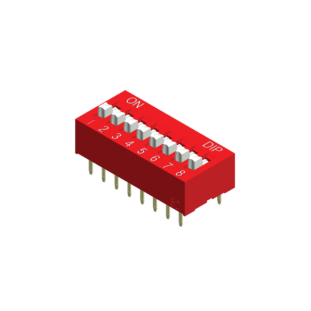
DHN Series Dip Switches
Position 2 ~ Position 10 Dip Switches
FEATURES
DHN series dip switches.
SPECIFICATION
Mechanical Life: 1, 000 operation cycles per switch.
Operation Force: 500gf max.
Operation Temp: -40°C to 85°C
APPLICATIONS
Home appliances and Computer peripherals.
SMD 10P DIP switch YESWITCH ELECTRONICS CO., LTD. , https://www.yeswitches.com


