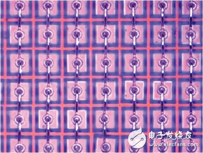
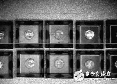
In recent years, the application of light-emitting diodes (LEDs) has been growing, covering a wide range of markets, including automotive lighting applications such as indicator lights, spotlights and headlights, camera functions such as display backlights and camera flashes, like LED displays. Consumer products such as backlights and projection systems, such as architectural lighting and signs, and many other applications. The LED has high brightness, high luminous efficiency and fast response. Incandescent lamps have been replaced in many ways due to their low energy consumption, long service life, low heat release and the ability to emit colored light. As the efficiency of LEDs continues to increase, the amount of lumens per watt that is generated continues to increase, and the use of LEDs for general illumination becomes more and more practical. For example, in 2003, a fluorescent tube equivalent to 3000 lumens required more than 1300 LEDs with an efficiency of 30 lumens per watt to achieve comparable results. However, by 2005, the number of LEDs required to obtain the same fluorescent tube illumination effect was reduced by 20 times, only about 50, and each LED had a luminous efficiency of 50 lm/W or higher and a luminous intensity of 60 lumens. LED lighting level There are four links in LED production, or four areas. The first link is called product link 0, which refers to the production device itself. The second link of product link 1 is a first-level package, which refers to the method of connecting the device to the power supply through chip bonding and wire bonding to form a surface mount package. The third link of product link 2 refers to the secondary package. Put multiple primary packages together to create the light output required for an external signal or outdoor lighting application. The fourth link of product link 3 is to systematically package the entire system or solution. The primary LED package includes a single LED and a complex LED matrix package. In a standard LED array, each LED is connected to a substrate electrode. LEDs can be handled separately or connected together. Most of this type of package utilizes an epoxy adhesive chip. For high-brightness LED applications, such as outdoor lighting or tail-projection screen illumination, a matrix-structured LED is required. In this configuration, the LEDs are arranged in close rows and columns to obtain as much light as possible. Figure 1 is an LED matrix diagram that together emits a large amount of lumens. The number and alignment of the LEDs requires good thermal conductivity of the die attach material to keep the LEDs as cold as possible. LED matrix diagram Figure 1 LED matrix diagram Matrix LED packages are the basis for many systems in production. Their recent popularity is due to the fact that this structure can get more lumens per watt of power. However, compared to single-chip packages, matrix LED packages pose significant challenges for chip bonding and wire bonding. High-brightness LED applications require maximum heat transfer to meet performance requirements. Package high brightness LED Matrix LED process steps include material preparation, chip pick and place, pulse reflow, cleaning, wire bonding, and testing. The following discussion will focus on pulse reflow (low temperature eutectic bonding) and wire bonding steps. An example is a 9 8 290 祄 LED matrix using AuSn bonding. The LEDs are electrically connected together in the column direction. The goal is to connect the LEDs to the substrate using metallurgical eutectic interconnects, placing the LEDs as close as possible based on component tolerances (approximately 1 mil of void). Figure 2 shows the 290-inch LED matrix. Adhering 290 micron LEDs to AuSn before wire bonding Figure 2 Attaching a 290 micron LED to the AuSn before wire bonding 18650 And 22650 And 26650 Cells Lithium Pro Batteries,Tesla Lithium Ion Battery,Lithium Ceramic Battery,Lithium Batteries For Sale Zhejiang Xinghai Energy Technology Co.,Ltd , https://www.headwayli-battery.com
